 Wenda Electronics
Wenda Electronics
Wenda Electronics
Engineered for high-density signal integrity, compact PCB layouts, and harsh environment durability.
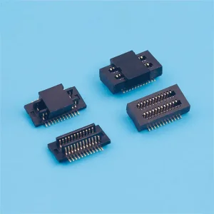
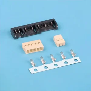
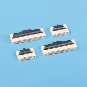
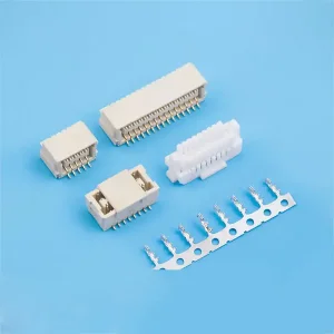
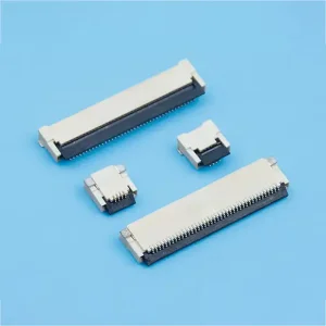
An in-depth whitepaper analysis on micro-pitch flexible circuits, materials physics, and advanced factory integration.
In modern electronic systems design—spanning 5G millimeter-wave mobile devices, 800V electric vehicle (EV) battery management modules, surgical medical robotics, and industrial IoT—the demand for space-saving, lightweight, and high-frequency signal transmission has positioned Flexible Printed Circuits (FPC) and high-density FFC/BTB Connectors as indispensable structural elements.
Unlike conventional rigid printed circuit boards (PCBs) or bulky wire harnesses, FPC cables provide multi-axis dynamic flexing, controlled impedance differential signaling, and extreme volumetric efficiency. Achieving high reliability in high-flex applications requires precise control over copper foil crystal structures (rolled-annealed vs. electro-deposited), dielectric substrate selection (Polyimide vs. Liquid Crystal Polymer), and ultra-precise connector contact mechanics (hinged flip-lock, push-down, butterfly latching).
Exploring next-generation dielectric substrates, micro-fine pitch geometries, and electromagnetic compatibility innovations.
As transmission frequencies push beyond 10 GHz towards 5G/6G frequencies, standard Polyimide (PI) substrates suffer from elevated dielectric constant (Dk ~3.5) and moisture absorption. The industry roadmap is migrating toward Liquid Crystal Polymer (LCP) and Modified Polyimide (MPI).
Driven by foldable displays and ultra-compact wearability, line width and line spacing (L/S) specs are transitioning from standard 50µm/50µm (2mil/2mil) down to 15µm/15µm micro-vias enabled by semi-additive processes (MSAP).
Micro-pitch connectors (0.3mm, 0.5mm, 0.8mm pitch) with zero-insertion-force (ZIF) hinged flip-locks are integrated to prevent trace delamination during high-speed automated placement.
Modern complex devices require multilayer FPCs (up to 8-12 layers) incorporating specialized Black EMI Shielding Films, silver paste overlay layers, and mesh ground plane structures.
This mitigates cross-talk and electromagnetic interference between radio-frequency (RF) front-ends and high-speed video processing circuitry.
| Substrate Material | Dielectric Constant (Dk @ 10GHz) | Dissipation Factor (Df @ 10GHz) | Moisture Absorption (%) | Max Continuous Operating Temp | Primary Application Target |
|---|---|---|---|---|---|
| Standard Thermoset PI | 3.4 – 3.6 | 0.010 – 0.015 | 1.8% | 260°C – 300°C | General Consumer Electronics, Lighting |
| Modified Polyimide (MPI) | 3.1 – 3.3 | 0.004 – 0.006 | 0.8% | 240°C – 280°C | 5G Sub-6GHz Smartphones, Wearables |
| Liquid Crystal Polymer (LCP) | 2.9 – 3.0 | 0.0015 – 0.0025 | 0.04% | 220°C – 260°C | mmWave 5G/6G Antenna, High-Speed Servers |
| High-Temp Fluoropolymer / PTFE | 2.1 – 2.4 | 0.0008 – 0.0012 | 0.01% | 260°C | Aerospace, Military Radar, Medical RF Probes |
Custom flexible interconnect engineering tailored to mission-critical operational environments.
Connectors act as comprehensive carriers of power transmission, safety protection, and intelligent interaction. In 800V ultra-fast charging platforms and Battery Management Systems (BMS), high-temperature resistant FPC harnesses replace heavy wire looms for cell voltage/temperature sensing, offering up to 60% weight reduction and flame-retardant safety matching IATF 16949 specs.
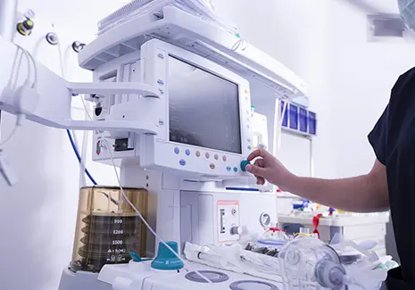
Medical interconnects demand high-density signal integrity, biocompatibility, and sterile reliability. FPC solutions are integrated into minimally invasive ultrasound probes, surgical endoscopes, and wearable patient monitors, utilizing gold-plated flip-lock connectors (0.5mm pitch) to maintain zero noise interference during micro-signal acquisition.
In foldable smartphones, laptops, and tablets, internal space is at a premium. Ultra-slim horizontal SMT connectors (1.0H/1.2H low profile) combined with high-flex dynamic FPCs withstand continuous mechanical bending across display hinges while enabling 4K/8K video transmission and fast charging power protocols.
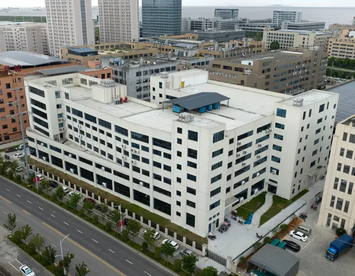
Inside Zhejiang Wenda Electronics Co., Ltd. — Automated precision tooling, high-speed SMT lines, and zero-defect quality control.
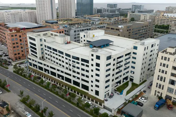
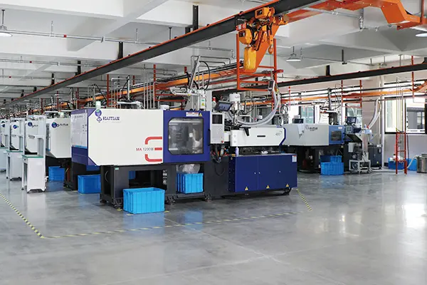
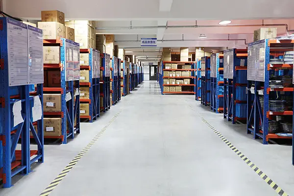
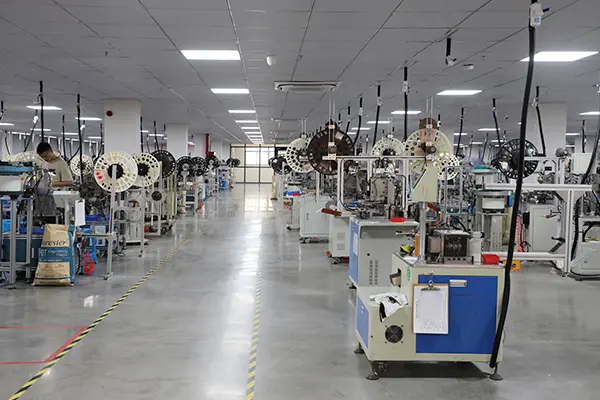
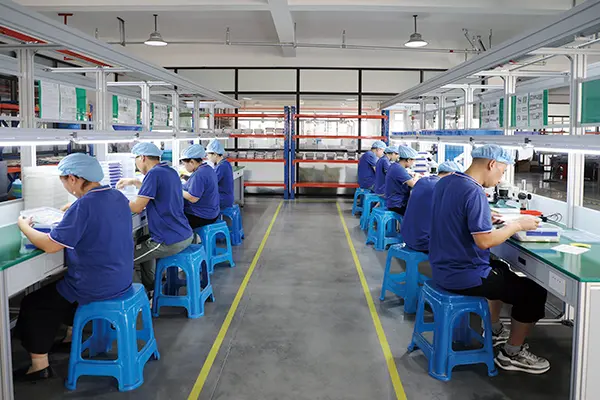
Founded in March 2007, Zhejiang Wenda Electronics Co., Ltd. is located in Yueqing Bay Lingang Economic Development Zone, Yueqing City, Zhejiang Province. Spanning a factory area of over 10,000 m² with a construction area exceeding 25,000 m² and employing over 500 skilled professionals, our smart manufacturing complex integrates complete R&D, tooling design, terminal stamping, plastic molding, and automated assembly.
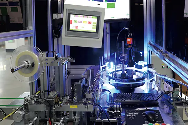
Our workshop floor hosts over 500 advanced production and testing equipment sets, including high-speed precision punching machines, precision injection molding equipment, automated multi-functional wire strippers, FFC automatic laminating/molding machines, and CCD visual inspection lines.
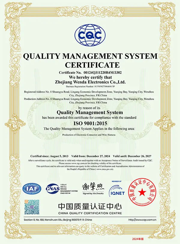
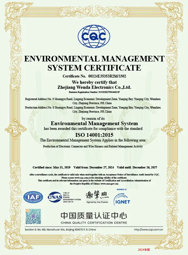
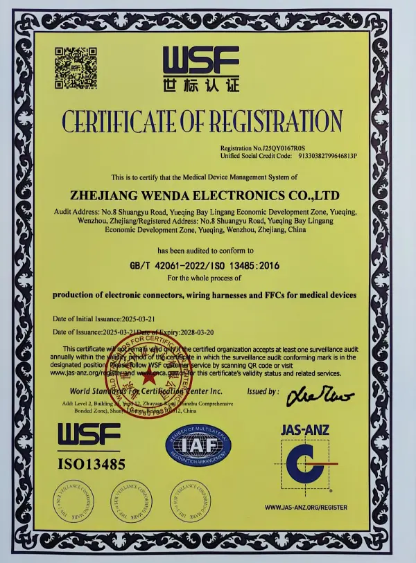
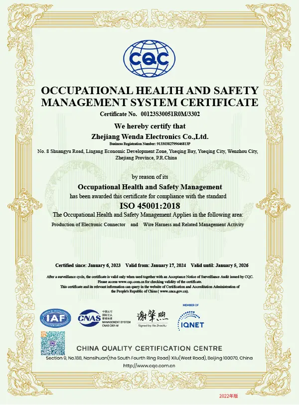
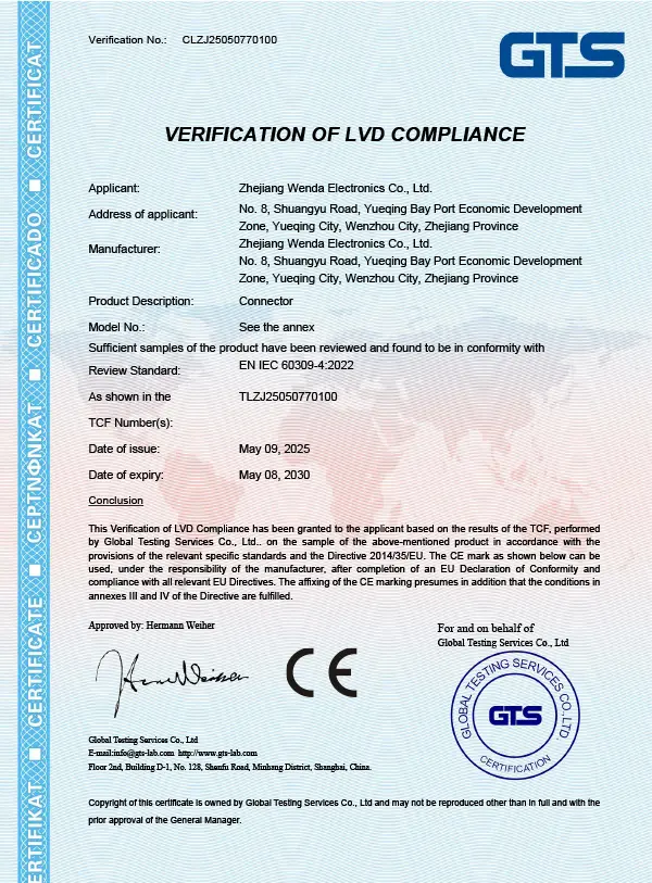
Certified management systems guaranteeing trace-level environmental compliance and multi-market authorization.
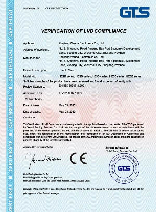
Zhejiang Wenda Electronics maintains rigorous operational standards to serve global automotive, industrial, and medical tier-1 vendors:
Every product batch undergoes non-destructive and analytical verification using top-tier laboratory instruments:
Strategic purchasing guidelines for OEM/ODM procurement leads and hardware architecture managers.
Eliminating Tier-3 distributor margins provides a 20% to 35% BOM cost reduction while establishing direct communication channels with our core mold design engineers.
Our R&D team delivers Design for Manufacturability (DFM) reviews within 24 hours, evaluating trace width geometry, pin count density, stiffener selection (FR4 vs. Stainless Steel), and automated SMT thermal profiles.
We support scaling hardware startups through high-volume mass production with Vendor-Managed Inventory (VMI) buffers and rapid sample dispatch in as fast as 48 hours.
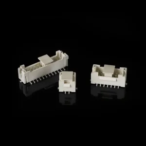
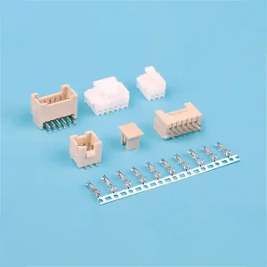
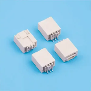
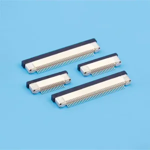
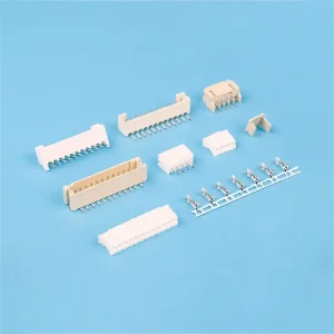
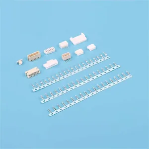
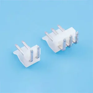
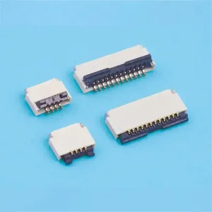
Explore our additional range of precision wire-to-board, FPC/FFC flip-lock sockets, and high-temp pin headers.
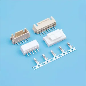
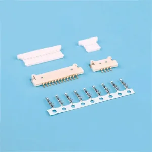
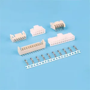
Expert insights on engineering selection, connector latching mechanisms, signal integrity, and manufacturing turnarounds.
Zero Insertion Force (ZIF) Flip-Lock sockets utilize a hinged actuator cover that lifts open. The FPC cable is inserted with zero friction, and closing the lever applies uniform contact pressure onto the gold-plated terminals. This prevents trace wear and allows up to 20+ mating cycles. In contrast, Drawer-Type (Non-ZIF/Slider) connectors require pushing the FPC directly into the contact cavity, which generates mechanical friction. Drawer types are ideal for low-cost, low-profile applications where re-mating is minimal.
Contact terminal gold plating (ranging from flash 1u" up to 15u" or 30u" selective gold) prevents contact oxidation, fretting corrosion, and micro-motion wear caused by vehicle vibration. For automotive BMS and ADAS systems certified to IATF 16949, a minimum of 3u" to 15u" gold plating over nickel underplating is recommended to maintain contact resistance below 30 mΩ across 1,000 continuous hours of thermal shock (-40°C to +125°C).
Yes. Our high-temperature connector series (such as PH2.0 and PHDC 2.0mm headers) are molded using high-thermal engineering thermoplastics like LCP, PA9T, or PPS. These materials feature a heat deflection temperature (HDT) exceeding 280°C, ensuring zero housing distortion or terminal misalignment during standard SAC305 lead-free reflow soldering profiles (peak temp 260°C for 10-20 seconds).
We implement a 100% inline CCD Visual Inspection System directly integrated into our high-speed automated packaging assembly lines. The vision systems check coplanarity (<0.10mm), pin pitch accuracy, terminal deformation, and housing flash in real-time. Defective units are automatically rejected, ensuring zero-defect tape-and-reel delivery ready for SMT pick-and-place feeders.
Our in-house toolroom designs and manufactures progressive stamping dies and injection molds. We offer custom contact layouts, tailored FPC reinforcement stiffeners (FR4, polyimide, aluminum, stainless steel), custom EMI shield bonding, and multi-branch jumper cable layouts. Prototype tooling lead time typically ranges from 7 to 14 business days.
Target differential impedance (e.g., 100Ω ±10% for HDMI/LVDS or 90Ω ±10% for USB 3.0) is determined by trace width ($w$), trace spacing ($s$), copper thickness ($t$), dielectric substrate height ($h$), and material dielectric constant ($\varepsilon_r$). Our engineering team uses 2D field solver modeling to deliver exact DFM stackup recommendations for your target layout.